In an era of computing power shortages, as demand for high-performance computing capabilities grows rapidly, the NVIDIA H100 GPU—an exceptional computing card—has become a highly sought-after commodity thanks to its outstanding performance in fields such as artificial intelligence, deep learning, and large-scale data processing.
However, the manufacturing process of the H100 GPU is no simple feat; it is accomplished through the coordinated efforts of multiple partner factories. Below, we have invited a product engineer from Yuanjie Computing to provide a detailed exploration of its manufacturing process.
First, NVIDIA’s engineering team is responsible for the GPU chip design, including circuit design, architecture design, and logic design. Through meticulous R&D and innovative design, they ensure the H100 GPU delivers outstanding performance and energy efficiency to meet a wide range of high-performance computing needs.
Next, the design specifications are handed over to TSMC, which utilizes its advanced 4N process technology to manufacture the logic chips. This is a critical step; as a global leader in semiconductor manufacturing, TSMC ensures the manufacturing quality of the H100 GPU through its superior process technology and efficient production capabilities.
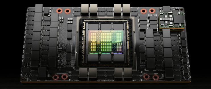
Meanwhile, South Korea’s SK Hynix plays a vital role by producing the HBM memory chips. HBM (High Bandwidth Memory) chips are a critical component of the GPU, enabling high-speed data transfer. SK Hynix manufactures three HBM memory chips on each side of the logic die and ships them to TSMC’s packaging facility.
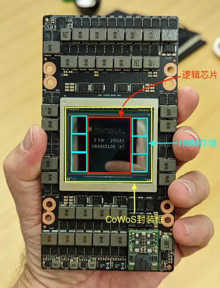
During the packaging phase at TSMC’s facility, the company employs advanced CoWoS technology to seamlessly integrate the logic chip with the HBM memory chips. This process combines one large chip with six smaller ones into a single, large package, enhancing the GPU’s performance and efficiency.
Subsequently, the packaged chips are sent to Foxconn’s contract manufacturing facility for further assembly. Foxconn is responsible for mounting the peripheral circuits and chips onto a circuit board, ensuring their integrity and reliability. This step is critical for achieving stability and performance, requiring the contract manufacturer to precisely assemble each chip and component with the aid of precision instruments.
Finally, the completed GPUs are sent to NVIDIA’s factories or partner testing facilities for rigorous testing and validation. These tests include functional testing, performance testing, stability testing, as well as temperature and power consumption testing, to ensure that every H100 GPU delivers the expected performance and quality.
In addition, NVIDIA works closely with global partners and its supply chain. These partners include chip foundries, packaging facilities, testing facilities, equipment suppliers, and raw material suppliers. Through collaboration with these partners, NVIDIA ensures a smooth and efficient production process.

Through this manufacturing process, the NVIDIA H100 GPU is brought to market flawlessly. The production of the NVIDIA H100 GPU requires rigorous design, manufacturing, packaging, and testing procedures. The coordinated efforts of numerous partner facilities ensure the exceptional quality and performance of the H100 GPU. However, its scarcity persists due to consistently high demand, while challenges in the supply chain and external factors cannot be overlooked.For various reasons, the H100 GPU has become a precious and hard-to-obtain commodity, comparable to gold. In this era of computing power scarcity, understanding the intricate craftsmanship behind the H100 GPU’s manufacturing will further reinforce people’s recognition of its exceptional value.
Yuanjie Computing Power – GPU Server Rental Provider
(Click the image below to visit the computing power rental introduction page)